Description of TPS6755
The TPS6755 is an adjustable inverter dc/dc converter capable of operating from inputs as low as 2.7V. The only external components required are an inductor, an output filter capacitor, an input filter capacitor, a reference filter capacitor, two resistors, and a Schottky rectifier. Provide an enable input to shut down the inverter when the output voltage is not required.
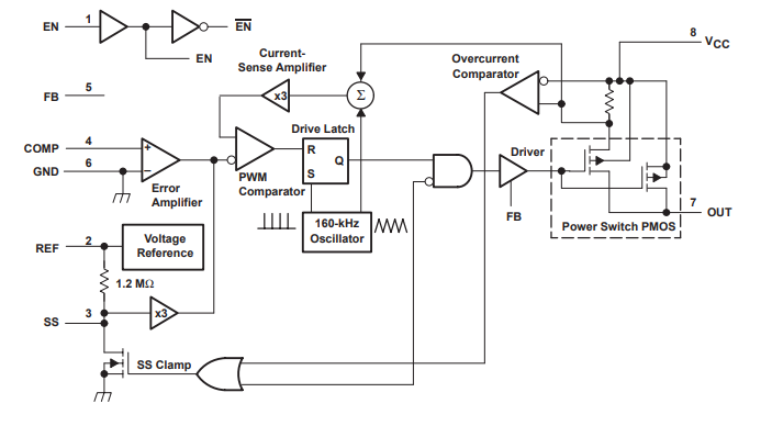
The typical supply current is 1.9 mA at no load and decreases further to 1-µA when the enable input is low. The device features a 160 khz current-mode pulse width modulation (PWM) controller with a P-channel MOSFET power switch. The grid driver uses a converter output to reduce the die area required to implement a 0.4-Ω MOSFET.
Soft boot is done by adding a small capacitor to the SS. The 1.22v reference can be used for external loads up to 125µA. Available in an 8-pin DIP or 8-pin SOIC package, the TPS6755 operates in the -40° free air temperature range and is suitable for board level dc/dc conversion in computer peripherals and battery-powered devices requiring high efficiency and low supply currents.
Typical circuit

Block diagram

Application circuit

Features
● 1-W Output (VCC ≥ 4.5V)
● 2.7-V to 9-V Input Operating Range
● 78% Typical Efficiency
● 160-kHz Fixed-Frequency Current-Mode
● PWM Controller
● EN Input Inhibits Operation and Reduces
● Supply Current to 1 µA
● The Output Voltage Limited to VO 12 V or less - VCC
● Soft Start
● 8-Pin SOIC and DIP Packages
● - 40°C to 85°C Free-Air Temperature Range
● Pin-for-Pin Compatible with MAX755