HMC900LP5E is a six-order, programmable bandwidth, fully calibrated, double low-pass filter. It has 0 or 10 dB input gain Settings, supports arbitrary bandwidth from 3.5 MHz to 50 MHz, and when calibrated, is accurate to +/-2.5% of the required bandwidth. It includes a 100 MHz bandwidth filter bypass option while preserving gain Settings and common-mode control.
The HMC900LP5E is packaged in a compact 5x5mm SMT QFN package that requires minimal external components and provides a low cost alternative to more complex switched discrete filter architectures. Integrated ADC drivers and externally controlled common-mode output levels further simplify system implementation.
Filter calibration for the HMC900LP5E can be done at any reference clock frequency from 20 to 80 MHz. Disposable programmable (OTP) memory offers unparalleled flexibility, allowing users to "set and forget" parameters such as gain and bandwidth Settings. The matched filter paths provide excellent orthogonal balance, making HMC900LP5E ideal for I/Q communication applications. The sixth-order Butterworth transfer function provides superior stopband suppression while maintaining a flat passband and minimal group delay variation.
HMC900LP5E Functional Diagram

HMC900LP5E Application Information
With unparalleled flexibility in today's complex multi-carrier and multi-standard systems, the HMC900LP5E offers an attractive alternative to other discrete filter solutions. Typical architectures that support multiple bandwidths either require a large board area or compromise filter selection at the expense of price or performance.
HMC900LP5E overcomes this limitation by allowing system designers to optimize the bandwidth of the desired signal, and also overcomes the matching problems of discrete filters in baseband signal processing. The matched dual filter path provides good gain and phase balance between the two channels, eliminating image problems caused by poor matching. The HMC900LP5E provides selectable gains and flexible output drivers to further improve system integration and reduce board area.
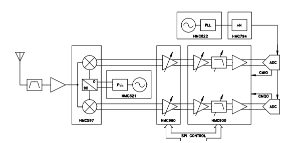
The following figure shows a typical receiving path block diagram of HMC900LP5E

Typical transmission path block diagram

Theory of Operation
The HMC900LP5E consists of the following function modules
(1) Enter the gain level
(2) Sixth order LPF
(3) Output driver
(4) RC calibration circuit
(5) Bias circuit
(6) Disposable programmable memory
(7) Serial port
(8) Built-in Self-Check (RC-BIST)
Input Gain Stage
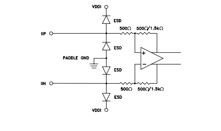
The HMC900LP5E input stage consists of a programmable 0 or 10 dB gain stage that drives 6 stages of LPF. Below is a block diagram showing the input impedance of channel I, similar to Channel Q.

Input phase block diagram
Features
● Low noise :12 decibels
● High linearity: output IP3 +30 dBm
● Pre-programmed and/or programmable bandwidth: 3.5 MHz to 50 MHz
● Integrated ADC drives the amplifier
● 3 dB bandwidth accuracy :±2.5%
● Six order Butterworth mode and phase response
● Automatic filter calibration
● Common-mode output level for external control
● Simplified interface
● Filter bypass option :100 MHz bandwidth
● SPI(Read/write serial port interface)
● 32 leads 5x5mm SMT package 25mm2
Applications
● Baseband filtering before or after A/D converter for point-to-point fixed wireless or base station transceivers (GSM/GPRS, WCDMA and TD-SCDMA)
● Integrated direct conversion receiver (DCR With blender and VGA
● Software defined radio applications
● Anti-aliasing and reconstruction filters
● Test and measurement equipment