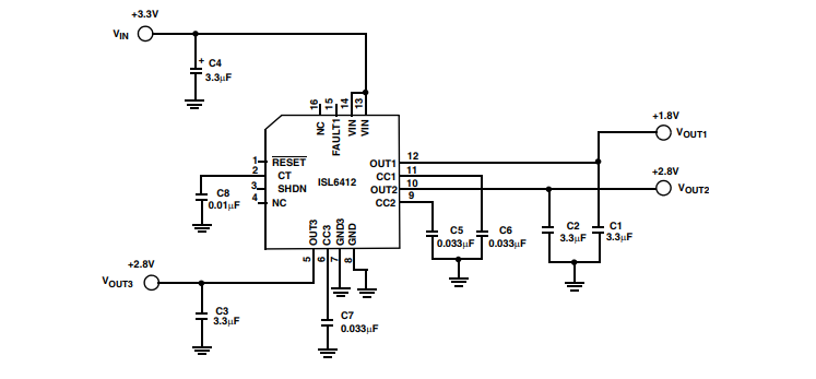
The ISL6412 is an ultra-low noise three-output LDO regulator with a microprocessor reset circuit optimized for powering wireless chipsets. The IC accepts input voltage ranges from 3.0V to 3.6V and offers three adjustable output voltages :1.8V (LDO1), 2.8V (LDO2) and another ultra-clean 2.8V (LDO3). On-chip logic provides sorting between LDO1 and LDO2 for the BBP/MAC and I/O supply voltage outputs. LDO3 has ultra-low noise, usually no more than 30 μV RMS, to aid VCO stability.
Typical Application Schematic

The high integration and thin Quad Flat No-lead (QFN) package make the ISL6412 ideal for many of today's small size industry standard wireless cards, such as PCMCIA, mini-PCI, and Cardbus-32. The ISL6412 uses an internal PMOS transistor as a path device.
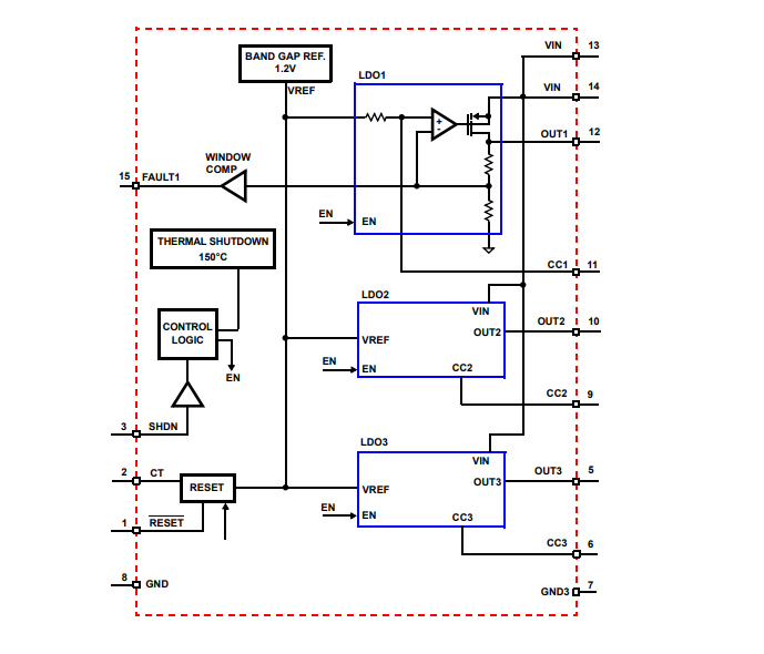
Functional Block Diagram

The ISL6412 also has an integrated reset function that eliminates the need for additional reset ics in WLAN applications. When the VIN supply voltage drops below a preset threshold, the IC asserts a RESET signal that holds it for some time after the VIN rises above the reset threshold set by the capacitor to GND. FAULT1 indicates that LDO1 is untuned.