CA3140E Introduction
The CA3140E is a BiMOS operational amplifier that combines PMOS and bipolar transistors for improved speed and efficiency. It features high input impedance, low input current, and operates on a wide supply voltage range of 4V to 36V (single or dual supply).
The op-amp is internally phase-compensated for stable unity gain operation and includes terminals for input offset voltage adjustment and optional external frequency compensation. With a common-mode input range extending 0.5V below the negative supply, it's well-suited for single-supply applications.
CA3140E Pinout

OFFSET NULL – Used for input offset voltage adjustment.
INVERTING INPUT (-) – The inverting input terminal of the op-amp.
NON-INVERTING INPUT (+) – The non-inverting input terminal of the op-amp.
V- – The negative power supply terminal.
OFFSET NULL – Another pin for input offset voltage adjustment.
OUTPUT – The op-amp’s output terminal.
V+ – The positive power supply terminal.
STROBE – Used to disable the output when pulled low.
CA3140E Symbol

CA3140E Footprint

CA3140E 3D Model

CA3140E Specification
| Parameter | Value |
| Supply Voltage (V+ to V-) | 4V ~ 36V |
| Gain Bandwidth Product | 4.5 MHz |
| Input Current | 10 pA |
| Output Current | 40 mA |
| Common Mode Input Voltage | 0.5V Below V- to V+ - 2V |
| Slew Rate | 9V/µs |
| Input Offset Voltage | 5 mV |
| Supply Current | 4mA |
| Phase Compensation | Internal |
| Short Circuit Protection | Yes |
| Operating Temperature Range | -55°C ~ 125°C |
| Package Type | 8-PDIP |
CA3140E Block Diagram

CA3140E Schematic Diagram

CA3140E Metallization Mask Layout
Dimensions in parenthesis are in millimeters and are derived from the basic inch dimensions as indicated. Grid graduations are in mils (10-3 inch). The photographs and dimensions represent a chip when it is part of the wafer. When the wafer is cut into chips, the cleavage angles are 57o instead of 90ο with respect to the face of the chip. Therefore, the isolated chip is actually 7 mils (0.17mm) larger in both dimensions.

CA3140E Features
• MOSFET Input Stage
- Very High Input Impedance (ZIN) -1.5TΩ (Typ)
- Very Low Input Current (Il ) -10pA (Typ) at ±15V
- Wide Common Mode Input Voltage Range (VlCR)
- Can be Swung 0.5V Below Negative Supply Voltage Rail
- Output Swing Complements Input Common Mode Range
• Directly Replaces Industry Type 741 in Most Applications
• Pb-Free Plus Anneal Available (RoHS Compliant)
CA3140E Applications
Ground-Referenced Single Supply Amplifiers in Automobile and Portable Instrumentation
Sample and Hold Amplifiers
Long Duration Timers/Multivibrators (µseconds-Minutes-Hours)
Photocurrent Instrumentation
Peak Detectors
Active Filters
Comparators
Interface in 5V TTL Systems and Other Low Supply Voltage Systems
All Standard Operational Amplifier Applications
Function Generators
Tone Controls
Power Supplies
Portable Instruments
Intrusion Alarm Systems
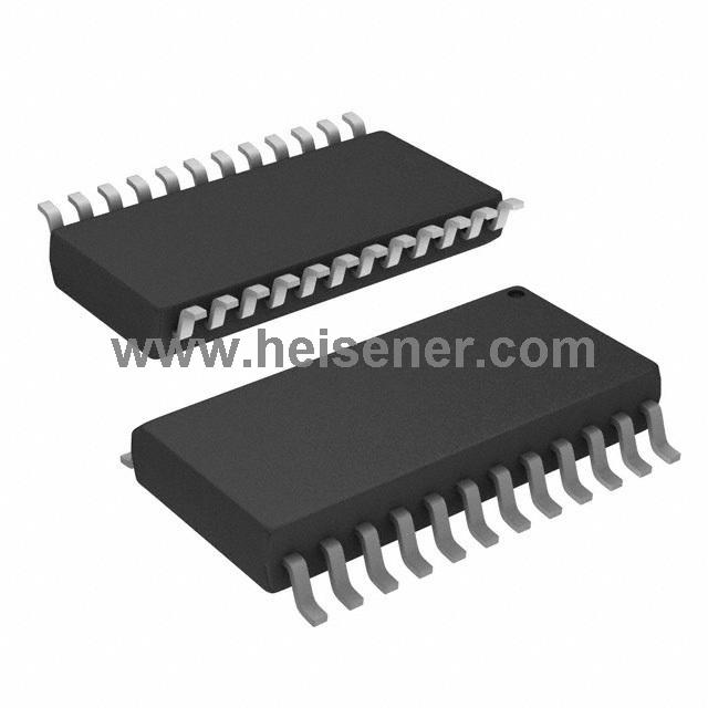
CA3140E Package
The CA3140E is available in an 8-PDIP Package, it is easy to integrate into standard through-hole circuit designs. This package provides durability, reliable connectivity, and ease of handling for prototyping and production. It makes proper heat dissipation and allows straightforward PCB mounting, suitable for a wide range of analog applications.

FAQs
What is the CA3140E?
The CA3140E is a high-performance BiMOS operational amplifier that combines PMOS and bipolar transistors, offering high input impedance, low input current, and wide voltage operation.
Does CA3140E require external compensation?
It includes internal phase compensation but allows an external capacitor for additional frequency roll-off if needed.
Does the CA3140E have short-circuit protection?
Yes, the output stage includes built-in protection against short circuits to ground or supply rails.