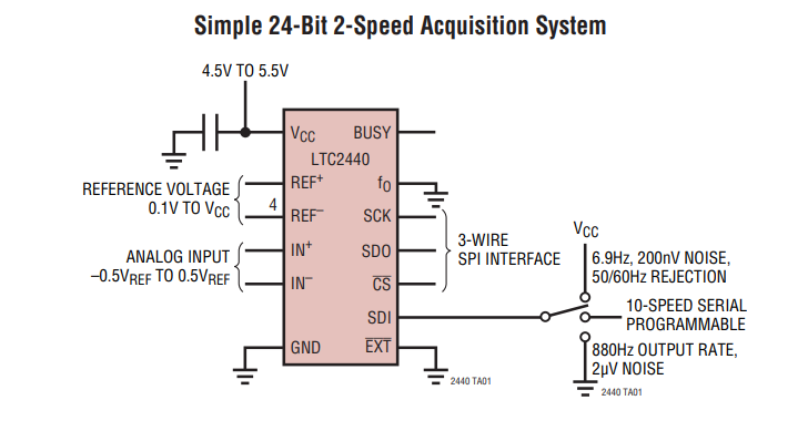
The LTC2440 is a high-speed 24-bit delay free ∆∑TM ADC with an INL of 5ppm and an offset of 5µV. It uses a proprietary delta-sigma architecture for variable speed and resolution without delay. Ten speed/resolution combinations (6.9Hz/200nVRMS to 3.5kHz/25µVRMS) are programmed through a simple serial interface.
Typical application

Alternatively, fast (880Hz/ 2μVRMS) or ultra-low noise (6.9Hz, 200nVRMS, 50/60Hz suppression) speed/resolution combinations can be easily selected by binding a single pin HIGH or LOW. Accuracy (offset, full range, linearity, drift) and power consumption are independent of the selected speed. Since there is no latency, speed/resolution changes can be made between transitions without degrading performance.
Functional block diagram

After each conversion cycle, the LTC2440 automatically enters low-power sleep. Increasing the duration of this sleep state reduces power consumption. For example, running at a 3.5kHz conversion speed, but reading data at a 100Hz rate requires an average current of 240µa (1.1mW), while reading data at a 7Hz output rate requires only 25µa(125µW). The LTC2440 communicates through a flexible 3 - or 4-wire digital interface that is compatible with the LTC2410 and offers a narrow 16-pin SSOP package.
Test circuit diagram
