The TLV5633 is a 12-bit voltage output digital-to-analog converter (DAC) with an 8-bit microcontroller-compatible parallel interface. Eight LSBS, four MSBS, and five control bits are written using three different addresses. The TLV5633 is suitable for a wide range of power supply voltages, operating from 2.7V to 5.5V.
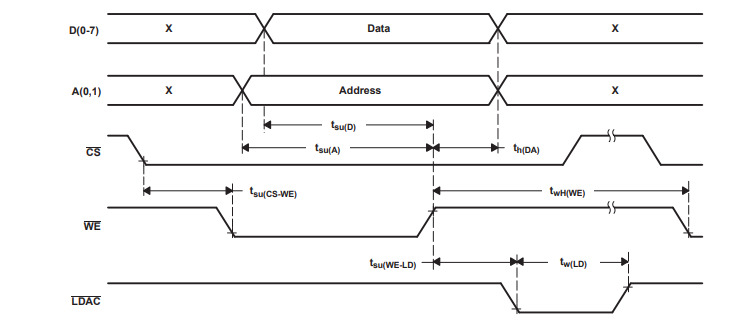
Time diagram

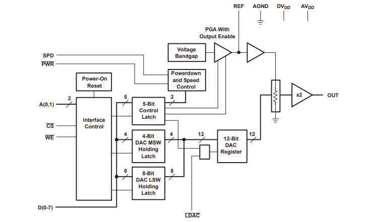
The resistance string output voltage is buffered by an x2 gain rail-to-rail output buffer. The buffer has a Class A (slow mode :AB) output stage to improve stability and reduce settling time. The DAC's programmable timing allows designers to optimize speed and power consumption. With its on-chip programmable precision voltage reference, the TLV5633 simplifies the overall system design. Internal guides can also be used as system guides due to their ability to provide a signal source up to 1ma.
Functional block diagram

The stability time and reference voltage can be selected by the control register. Implemented using a CMOS process, the device is designed for single-power operation from 2.7V to 5.5V. It is available in 20-pin SOIC and TSSOP packages in standard commercial and industrial temperature ranges.